ReRAM revolutionizes edge computing with 100x faster reads, 20x less energy than flash, enabling AI processing and years-long IoT device operation without recharging.
Drivetech Partners
Resistive random-access memory (ReRAM) is emerging as the cornerstone technology that's fundamentally reshaping low-power edge computing and Internet of Things applications. This revolutionary memory technology addresses critical limitations of traditional memory solutions at advanced process nodes while delivering unprecedented energy efficiency, speed, and integration capabilities essential for next-generation connected devices.
Key Takeaways
- ReRAM delivers 100x lower read latency and 1000x faster write performance than flash memory
- Consumes 20x less energy than NAND flash with 64pJ/cell program energy consumption
- Enables monolithic integration with CMOS logic for single-chip IoT system solutions
- Facilitates AI processing at the edge through compute-in-memory architectures
- Industry collaborations like EMASS and Weebit Nano are accelerating commercialization for ultra-low power applications
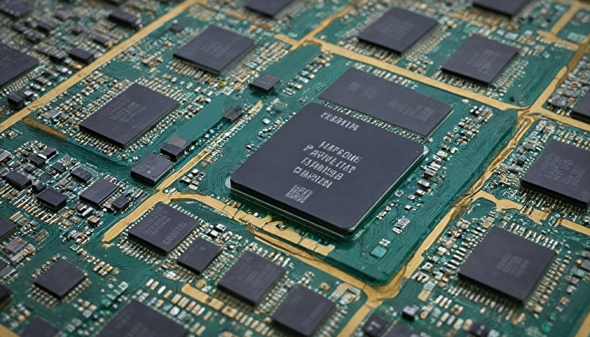
Technical Superiority of ReRAM Over Traditional Memory
ReRAM represents a quantum leap forward in memory technology, offering performance characteristics that make it ideal for edge computing applications. Unlike conventional memory technologies, ReRAM achieves 100x lower read latency and an astonishing 1000x faster write performance compared to flash memory. These speed improvements translate directly to more responsive and capable edge devices.
Energy efficiency stands as another dramatic advantage, with ReRAM consuming just 64pJ/cell for program operations—a 20x improvement over NAND flash technology. This remarkable efficiency is possible because ReRAM uses a fundamentally different approach to data storage based on resistance states rather than stored charge.
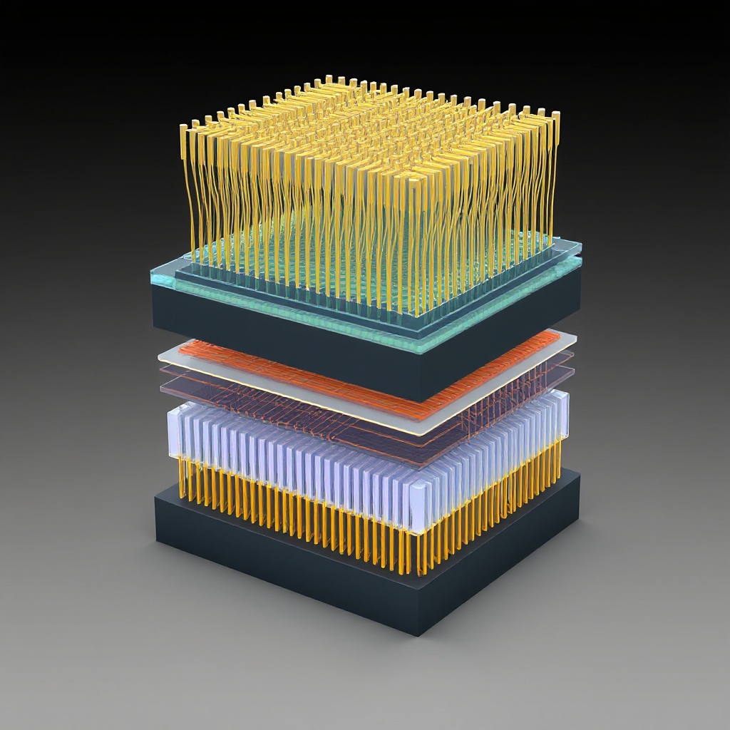
The technology's bit-alterable, erase-free operation eliminates the complex block erase cycles required by flash memory. ReRAM maintains stable performance across wide temperature ranges and doesn't degrade at smaller process nodes, with proven potential to scale below 10nm. The switching mechanism relies on electric fields with filamentary nanoparticles, using non-conductive amorphous silicon (a-Si) as the switching material.
Manufacturing and Integration Advantages Driving Adoption
The simplified device structure of ReRAM uses CMOS-friendly materials and standard manufacturing processes, enabling straightforward integration with existing semiconductor fabrication techniques. This compatibility allows ReRAM to be integrated with CMOS logic on the same process node, creating opportunities for new memory-centric architectures.
Low-temperature back-end-of-line process integration represents another significant advantage. Multiple ReRAM layers can be stacked between metal routing layers to increase memory density without substantially increasing chip size. The technology can be manufactured in existing CMOS fabs without specialized equipment, reducing implementation barriers.
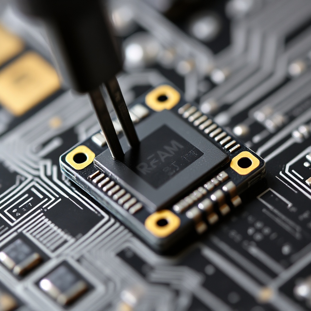
These manufacturing advantages support monolithic integration for single-chip IoT system solutions, making ReRAM a cost-effective alternative to traditional embedded memory technologies. The result is smaller, more capable chips that can combine memory, processing, and even analog/RF components on a single die.
Energy Efficiency Transforming IoT Device Capabilities
For IoT applications, energy efficiency often determines what's possible. ReRAM enables local data buffering, reducing the frequency of power-hungry cloud data transmission. This local storage and processing capability eliminates the need for expensive controllers or complex memory management schemes typically associated with flash memory.
The integration capabilities allow logic processing, analog, and RF components to coexist on a single efficient chip. This consolidation, combined with ReRAM's inherent power savings, enables IoT devices to operate for years without battery recharging—a critical requirement for remote or inaccessible deployment scenarios.
Power consumption reductions come from multiple sources: fewer I/O operations, shorter code execution times, and the ability to implement intelligent power management policies that are essential for extending battery life. The technology is approximately 20x more energy-efficient than traditional NAND flash, creating opportunities for entirely new categories of ultra-low-power devices.
Industry Collaboration Accelerating ReRAM Commercialization
The recent partnership between EMASS and Weebit Nano, announced on March 6, 2025, demonstrates the growing commercial momentum behind ReRAM technology. The collaboration focuses on edge AI applications, combining Weebit's ReRAM with EMASS' ultra-low power AI system-on-chip at a 22nm process node.
A live demonstration planned for the embedded world 2025 Conference & Exhibition will showcase the technology's capabilities. Notably, EMASS transitioned from MRAM to ReRAM technology specifically to better support next-generation systems with unprecedented performance and efficiency requirements.
This collaboration aims to develop a monolithic edge AI solution that pushes the boundaries of what's possible in power-constrained environments. Beyond this specific partnership, leading foundries are increasingly integrating ReRAM technology as their embedded non-volatile memory solution of choice, particularly for applications below the 28nm node where traditional embedded memories face significant challenges.
Neuromorphic Computing and AI at the Edge
ReRAM's unique properties make it ideal for enabling compute-in-memory architectures that dramatically improve AI processing efficiency. By allowing computations to occur directly within the memory array, these architectures eliminate the power-hungry data transfers between separate memory and processing units that dominate energy consumption in conventional systems.
The technology supports event-based sensors like retinomorphic cameras for energy-efficient operations, mirroring how biological systems process information. ReRAM facilitates online, continuous learning in edge devices without requiring cloud connectivity, creating truly autonomous intelligent systems.
This approach creates distributed intelligence across what technologists call the "continuum of computing" from cloud to edge. The physical properties of ReRAM cells even mimic biological neural structures, enabling more efficient machine learning implementations and real-time inference in power-constrained environments.
Real-World Applications Across Multiple Industries
The practical applications for ReRAM span numerous industries and use cases. In smart homes, cities, and buildings, energy-efficient sensors and controllers can operate for years without maintenance. Healthcare applications include wearable monitoring devices and point-of-care diagnostic equipment that require both low power consumption and fast response times.

Automotive systems benefit from ReRAM's instant wake-up capabilities and low power consumption, while industrial automation and monitoring applications leverage its reliability in harsh environments. Consumer electronics, particularly wearable devices, gain extended battery life and improved performance.
ReRAM also enables innovative security applications through physical unclonable function (PUF) keys, creating hardware-based security features that are difficult to compromise. Always-on sensing applications for predictive maintenance and anomaly detection become practical with the dramatic reduction in power requirements.
Future Outlook and Market Potential
The market for ReRAM in IoT applications is expected to grow significantly as manufacturing costs decrease with wider adoption. The technology addresses fundamental limitations at advanced process nodes below 28nm where traditional embedded memory struggles with physics-based constraints.
ReRAM is enabling entirely new device categories that weren't previously possible due to power constraints. The growing ecosystem of IP providers, chip designers, and system integrators supporting ReRAM indicates strong industry confidence in its future.
Industry analysts project ReRAM will become the standard embedded non-volatile memory for IoT and edge AI applications over the next decade. Beyond just memory replacement, ReRAM is creating opportunities for new compute paradigms and architectures specifically optimized for edge deployment, potentially reshaping how we think about distributed computing infrastructure.

Sources
Weebit Nano - EMASS and Weebit Nano Collaborate on Ultra-Low Power Edge AI Demonstration Using ReRAM
IT Brief Asia - Weebit and EMASS reveal ReRAM edge AI advancements
Crossbar Inc - Internet of Things
Embedded Computing - Cutting IoT Power Consumption with Embedded ReRAM
Crossbar Inc - ReRAM Advantages
Semiconductor Digest - EMASS and Weebit Nano Collaborate on Ultra-Low Power Edge AI Demonstration Using ReRAM