
Siemens' Innovator3D IC revolutionizes semiconductor design with unified digital twin technology, enabling efficient 2.5D/3D chiplet integration and early multiphysics analysis.
Drivetech Partners
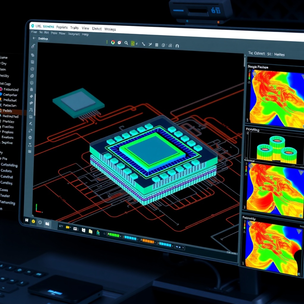
Siemens' Innovator3D IC cockpit represents a transformative approach to semiconductor design through its unified digital twin data model and system technology co-optimization methodology for advanced 2.5D/3D IC design. This award-winning solution, announced at DAC 2024 in San Francisco, enables efficient "shift-left" processes for chiplet and ASIC integration by providing comprehensive planning, prototyping, and multiphysics analysis capabilities from early design stages through manufacturing.
Key Takeaways
Digital twin technology accelerates semiconductor design with 80% of companies now employing digital twins across industries
Built on IMEC-developed STCO methodology for comprehensive prototyping, planning, and manufacturing hand-off
Hierarchical device planning manages the massive complexity of advanced designs with millions of pins
Integrated multiphysics analysis tools enable early identification of design issues before implementation
Direct integration with Siemens Xcelerator portfolio and support for third-party solutions enhances design flexibility

Innovator3D IC: Revolutionizing Advanced Semiconductor Design
Siemens' Innovator3D IC cockpit signals a major advancement in semiconductor package design, earning the 2025 3D InCites Technology Award. Announced during DAC 2024 in San Francisco by AJ Incorvaia, Senior VP of Electronic Board Systems Group at Siemens EDA, the solution is scheduled for release later in 2024. It serves as a core technology for heterogeneous integration of ASICs and chiplets using advanced 2.5D and 3D technologies.
The semiconductor industry faces increasing challenges as designs become more complex and market demands grow. Innovator3D IC responds to these challenges by providing a unified environment for constructing complete semiconductor package digital twins, facilitating early risk identification and creating a predictable path for planning and integrating complex chiplet-based designs.
The Digital Twin Revolution in Semiconductor Design
Digital twins have transformed product development across industries, with 80% of companies now employing this technology according to Cap Gemini research. The semiconductor industry, expected to reach a $1 trillion market value by 2030, has embraced digital twins to accelerate design cycles and improve decision-making.
Innovator3D IC leverages a unified data model specifically built for design planning, prototyping, and predictive analysis. This model serves as a secure design IP digital thread conduit that drives implementation through to manufacturing. Digital twins now apply at multiple levels—from individual chips through sub-systems to complete system-level designs.
The strategic value of digital twins in semiconductor design includes:
Accelerated understanding of product behavior
Enhanced decision-making using real-time and historical data
Improved collaboration between design teams
Reduced time-to-market for complex designs
Decreased development costs through virtual prototyping
System Technology Co-Optimization (STCO) Methodology
At the heart of Innovator3D IC lies the IMEC-developed STCO methodology, which serves as the core architectural foundation. This methodology is utilized throughout the entire design workflow: prototyping, planning, design, sign-off, and manufacturing hand-off.
STCO extensively leverages AI technology for co-optimization of semiconductor designs. The process concludes with comprehensive verification and reliability assessment, enabling early risk identification and avoiding costly downstream rework. This approach supports rapid what-if exploration of design alternatives, letting engineers quickly evaluate multiple options before committing to implementation.
The STCO methodology provides several key advantages:
Holistic approach to semiconductor design optimization
Seamless transitions between design stages
AI-driven optimization of critical design parameters
Risk mitigation through early verification
Efficient exploration of design alternatives
Managing Complexity Through Hierarchical Device Planning
Modern semiconductor designs can involve millions of pins and interconnections. Innovator3D IC handles this massive complexity through hierarchical device planning, implementing geometrically partitioned regions with specific elaboration attributes.
This approach allows critical updates to be quickly implemented through targeted regional analysis. It prevents excessively long execution times while maintaining accuracy across the design. The system optimizes chiplet interfaces and pin assignments via hierarchical interface route path planning and features rules-based connectivity optimization for complex interfaces.
The hierarchical planning approach delivers several benefits:
Precise control over region-specific design rules
Efficient management of design iterations
Optimized execution time for large designs
Improved interface optimization between chiplets
Enhanced connectivity management for complex designs
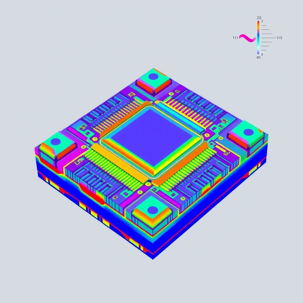
Integrated Multiphysics Analysis for Shift-Left Design
Innovator3D IC includes unified tools for power, signal, thermal, and mechanical stress analysis. This integrated approach delivers PPA (power, performance, area) and cost-optimized designs while enabling early identification of design issues before implementation.
The platform's integrated verification and reliability assessment facilitates what-if explorations to evaluate design alternatives quickly. This shift-left approach prevents costly and time-consuming downstream rework or suboptimal results by addressing potential issues early in the design cycle.
Key multiphysics analysis capabilities include:
Comprehensive thermal analysis of chiplet interactions
Signal integrity verification for high-speed interfaces
Power distribution network optimization
Mechanical stress prediction for reliability assessment
Integrated analysis for cross-domain optimization
Siemens Ecosystem Integration and Tool Compatibility
Innovator3D IC features direct integration with the extensive Siemens Xcelerator technology portfolio. It drives implementation using multiple Siemens tools including Aprisa digital IC place and route, Xpedition Package Designer, Calibre 3DThermal, NX for mechanical design, Tessent Test, and Calibre 3DSTACK.
The platform also supports third-party point solutions to accommodate customers' existing design flows. This flexibility has earned industry recognition, with Intel Foundry's Suk Lee endorsing Innovator3D IC as "an important design technology component for our advanced integration platforms."
The integration advantages include:
Seamless data transfer between design stages
Consistent design rules application across tools
Preservation of design intent throughout the flow
Compatibility with existing customer investments
Future-proof design methodology
Future Outlook and Industry Standardization
The semiconductor industry needs standardized digital twin framework architecture for better interoperability. Enhanced reliability, synchronization, and security through standardization efforts will drive the next wave of design efficiency.
The application of digital twins is expanding across hardware and software domains, transforming how complex semiconductor packages are designed and manufactured. There's growing adoption in 2.5D and 3D chiplet-based designs for next-generation computing as the industry recognizes the value of integrated design environments.
Looking ahead, we can expect:
Further AI integration into design optimization
Expanded digital twin capabilities across the supply chain
Increased standardization of digital twin interfaces
Greater automation of design decisions
More seamless integration between design and manufacturing
Key Benefits for Advanced Semiconductor Design
Innovator3D IC streamlines the "shift-left" process of prototyping, planning, and analysis through its unified cockpit environment for constructing complete semiconductor package digital twins. The platform enables early risk identification and mitigation before physical implementation.
Design teams can achieve optimized PPA (power, performance, area) and cost metrics through the platform's hierarchical approach to manage massive complexity of advanced designs. This creates a predictable path for planning and heterogeneous integration of ASICs and chiplets, essential for next-generation computing architectures.
The combined benefits make Innovator3D IC a transformative solution for semiconductor companies looking to maintain competitive edge in an increasingly complex design landscape.
Sources
blogs.sw.siemens.com - Siemens Introduces Innovator3D IC
newsroom.sw.siemens.com - Innovator3D IC
resources.sw.siemens.com - Fact Sheet Innovator3D IC
semiwiki.com - Siemens Provides a Complete 3D IC Solution with Innovator3D IC
blogs.sw.siemens.com - Innovator3D IC Wins 2025 3D InCites Award